Switch-mode power supply 12 V / 50 W with UC3843
I found a discarded power-supply PCB in electronic waste, it was probably a laptop power supply. Some components were missing. As always, I took it apart, but I felt like learning something new and making use of the switching transformer. I know that laptop power supplies can deliver interesting currents. The result is this design - a supply that gives 12 V and around 50 W (a little over 4 A).
In this article I’m publishing my findings, the schematic, the PCB layout, and also a description of the components and what each of them does. It’s quite difficult to get hold of such reliable and coherent information, since all the "blogs" just copy from each other: incomplete and completely wrong information, schematics with errors and incorrect component values. The main thing is that all the ads show up (not for me, I’ve got uBlock) and the “blog author” gets effortless profit...
The original power supply also had PFC and was controlled by some exotic IC, for which there is a datasheet with a schematic, but no component values. I decided to use the well-known UC3843A IC and omit the PFC.
For anyone who decides to take inspiration from this circuit, obligatory warning - when working with mains voltage, follow all safety procedures and be extremely careful. This construction is published for informational purposes and you do everything at your own risk. If you don’t have experience, better leave it alone. Mains electricity kills!
The transformer
The transformer is marked EDAC E307207 and there is absolutely no information available about it. It has one primary winding, one secondary winding, and one auxiliary winding. I measured their inductances, and AI calculated the turn ratios and an expected load current of around 50 W.
Here are the winding parameters I measured at different frequencies:
| Winding | Inductance | Q | Frequency |
| Primary | 305 μH | 22 | 1 kHz |
| 303 μH | 104 | 10 kHz | |
| 303 μH | 116 | 100 kHz | |
| Auxiliary | 10 μH | 0.538 | 1 kHz |
| 9.9 μH | 5.11 | 10 kHz | |
| 9.8 μH | 38.7 | 100 kHz | |
| Secondary | 6.2 μH | 1.8 | 1 kHz |
| 6.2 μH | 18.3 | 10 kHz | |
| 6.2 μH | 129 | 100 kHz |
Since Q increases with frequency, this transformer “feels best” in the range of the higher tens of kHz. According to AI, it’s better to have some margin in the operating frequency and 80 kHz is commonly chosen, so I went with that as well.
Schematic
Click to show the large version.
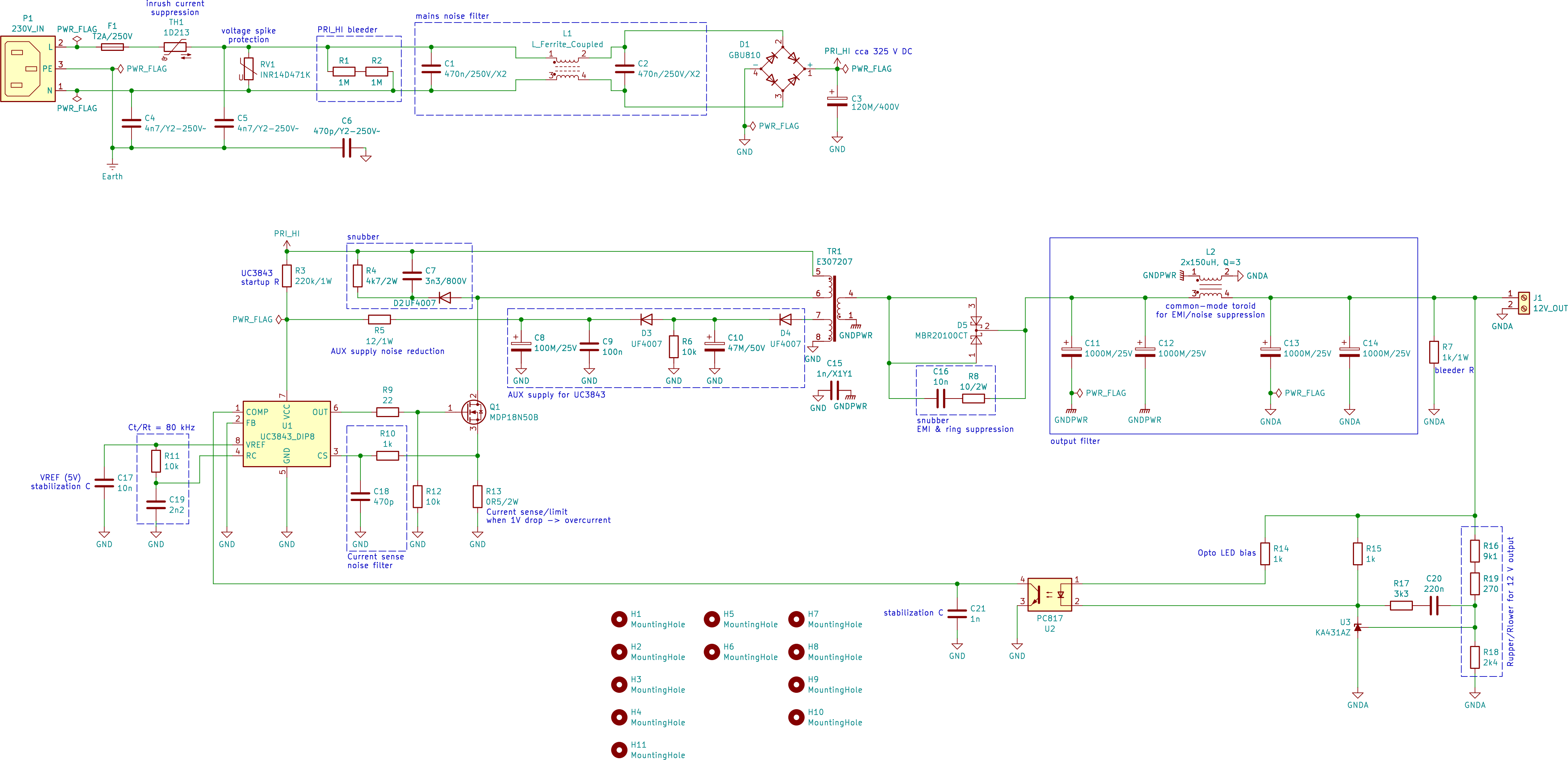
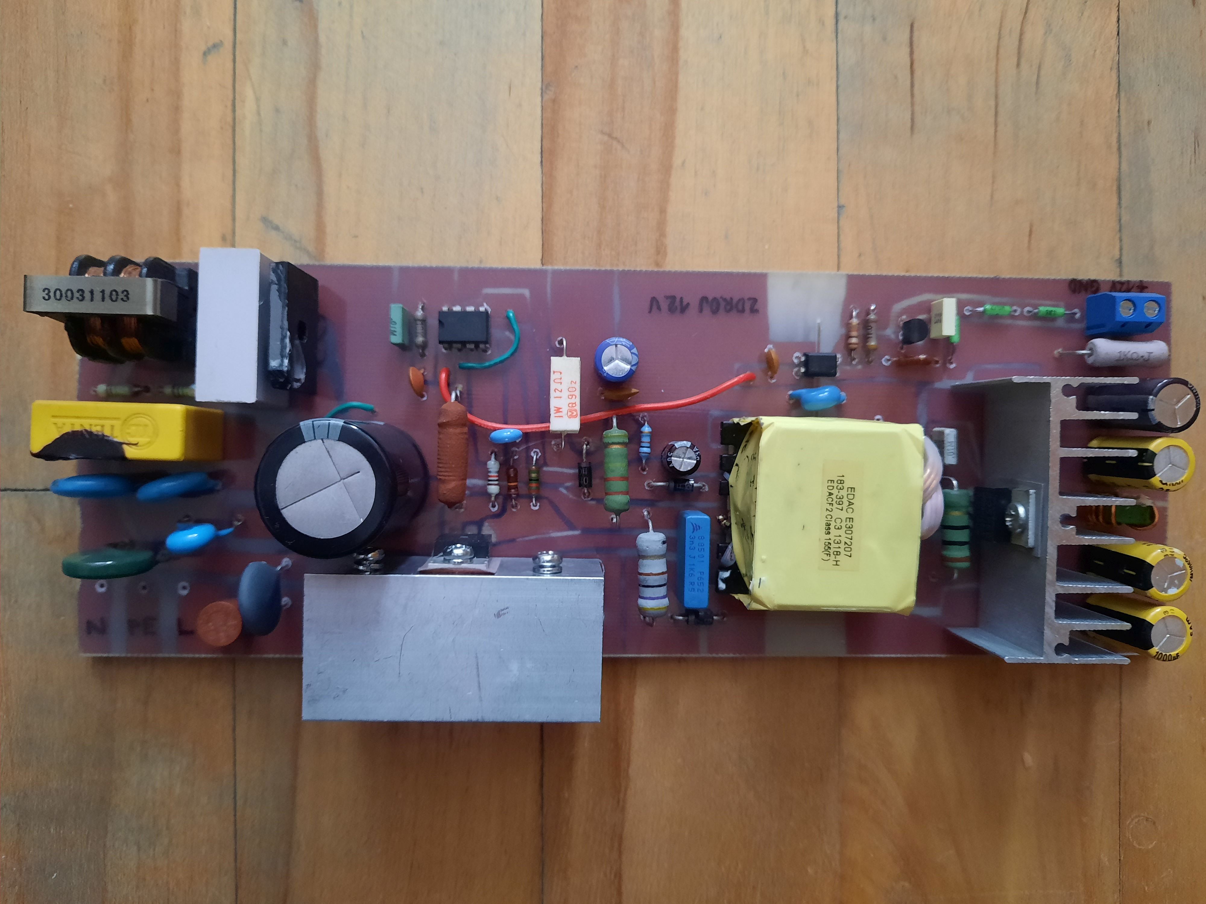
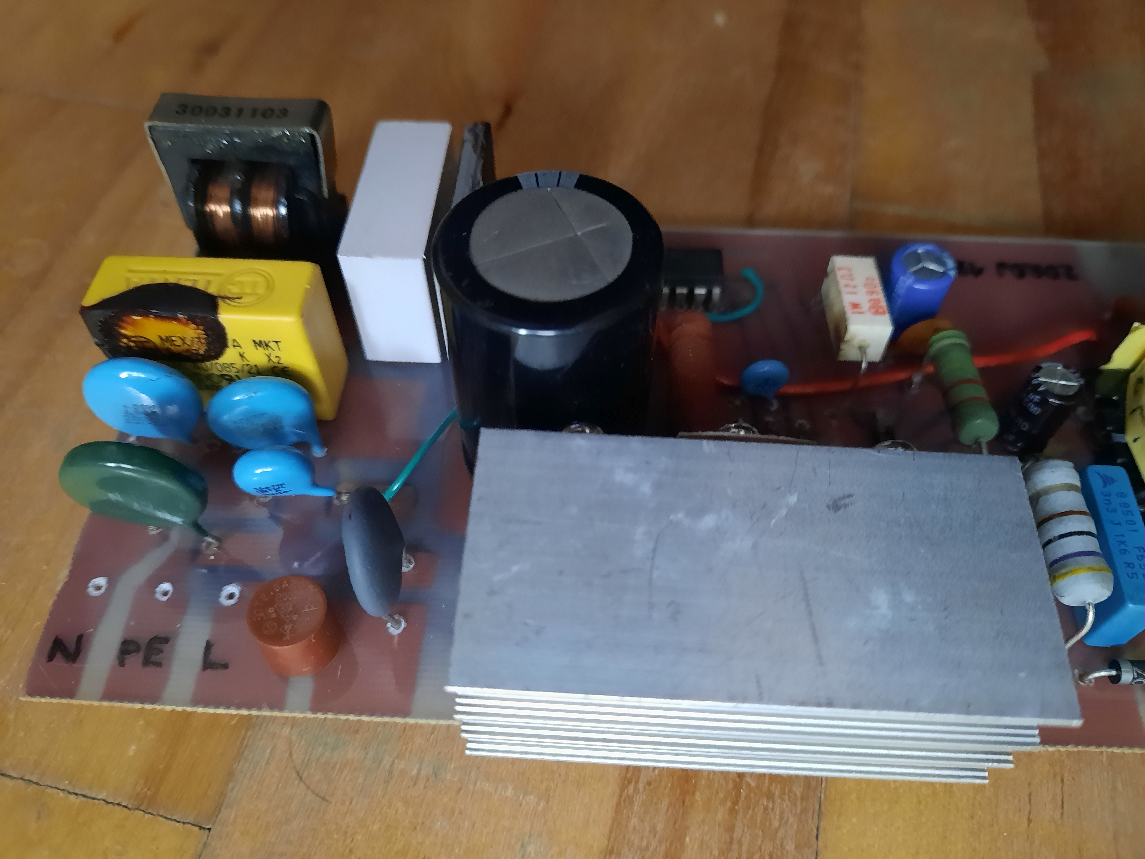
It's a standard switch-mode power supply circuit (SMPS) with UC3843A. At the input there is a fuse, a varistor against voltage spikes from the mains, a thermistor to limit inrush current at power-on, a few Y-type safety capacitors, and two resistors to discharge the main capacitor after the supply is disconnected. Components C1, L1, C2 form a filter that prevents noise from the supply from leaking back into the mains. L1 is a common EMI choke with two windings on a shared core, the kind that is (or at least should be) found in every SMPS. This is followed by a diode bridge rectifier and the main smoothing capacitor.
After connecting to the mains, a DC voltage of about 325 V appears on C3 (depending on what's in the mains). The UC3843A IC is powered for a short moment through resistor R3, and when the oscillator in it starts up at 80 kHz (frequency set by R11 and C19), the MOSFET on its output starts switching the primary voltage together with the oscillator, and the desired voltages appear on the transformer’s auxiliary and secondary windings.
The auxiliary winding is connected to a rectifier and smoothing stage whose output is about 15 V. From that moment on, this voltage is used as the supply voltage for the UC3843A. In its path there is also R5, whose role is to filter spikes (the value is not critical, from 4.7 to 68 Ω). Some designs also show a zener diode, but that is already integrated in the IC itself, so in my opinion it's unnecessary.
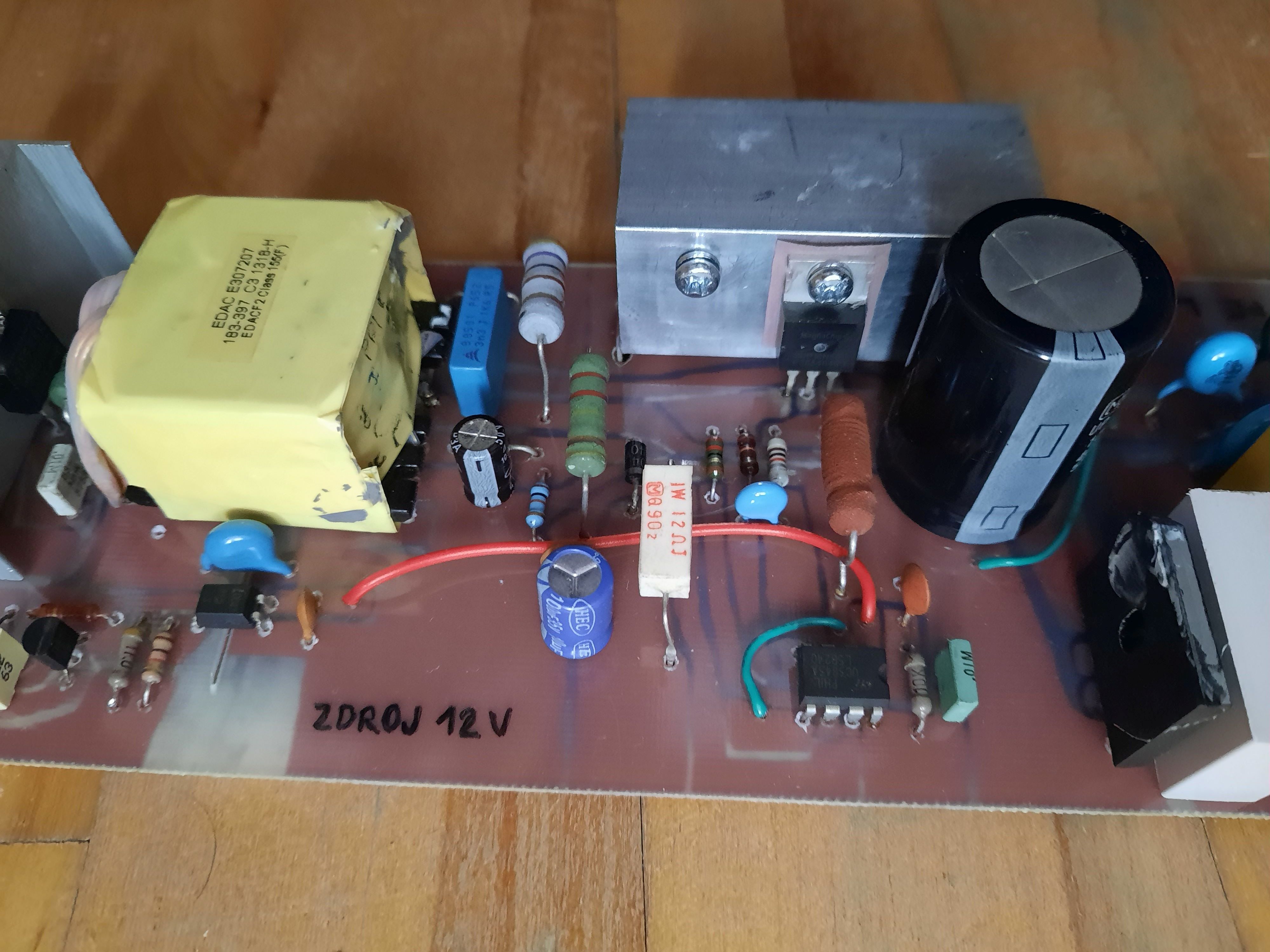
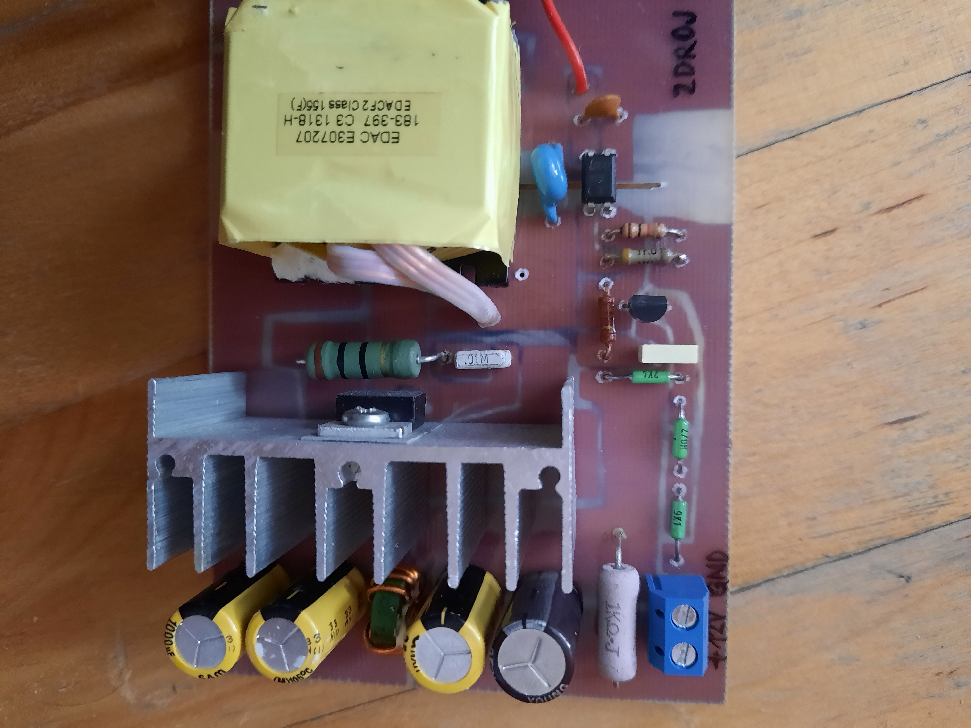
R13 sets the current limit - if there is a 1 V drop across it, the IC switches the supply off. The MOSFET is MDP18N50B taken from the original salvaged supply, but any similar MOSFET such as IRF840 will work. It must be mounted on a heatsink.
Components D2, R4, C7 act as a so-called snubber; they protect the MOSFET from excessively high voltage and reduce its stress. However, R4 burns off energy, so choosing the values of the snubber components is practically a science and a compromise. I took inspiration from the values used in another design with similar supply parameters.
Capacitor C15 is connected between primary and secondary ground, a good practice. It was also present in the original recycled design, so I kept it. It usually has a value from 1 nF to 4.7 nF and must have special safety ratings to maintain insulation strength between the primary and secondary side. To improve isolation, there is also air gap in the PCB.
On the secondary side, around the Schottky dual diode, there is a capacitor and resistor in series - C16 and R8. This is again a snubber that helps the transformer. In my case, the spikes on the output (noise ripple) dropped to a third when I added this snubber. The component values are again some commonly chosen and recommended ones. R8 heats up.
The secondary winding thus goes through the rectifying dual diode into a CLC filter. Instead of a simple inductor (as is often used in these supplies), there is a green toroid with two windings, and both the output voltage and ground pass through it - again a concept taken from the original design. The capacitors must of course be low-ESR.
R7 serves to discharge the output capacitors when the supply is disconnected from the mains. The output voltage is sampled for the TL431, which controls the optocoupler as feedback to the primary side so that the IC maintains a constant output voltage. R16+R19 and R18 (their ratio) determine the specific value of the output voltage that is to be maintained. By changing them, it is possible to adjust the output voltage within a small range. Even a small change in the resistance of these resistors causes a significant change in the output voltage, and therefore these resistors must have precise values (for example, built up from several resistors, as here).
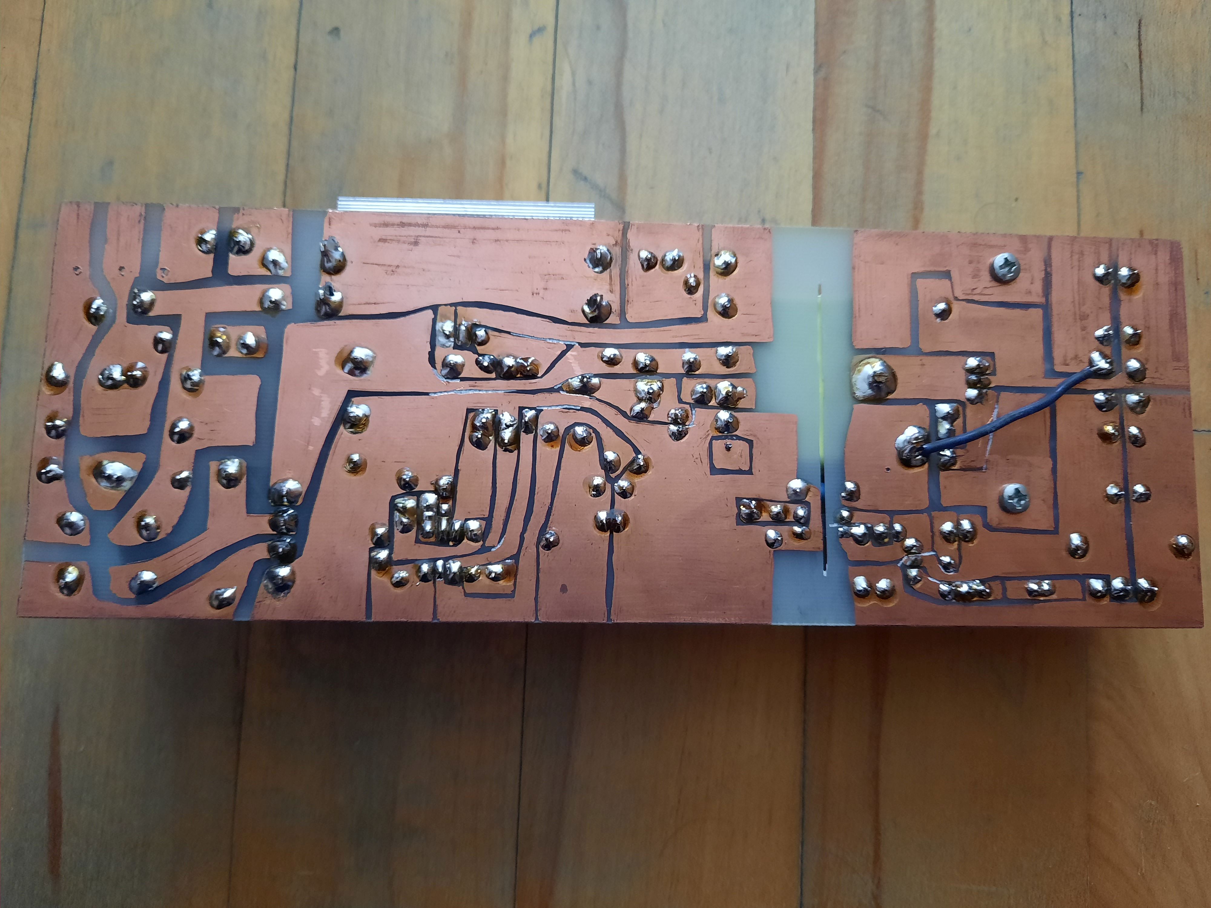
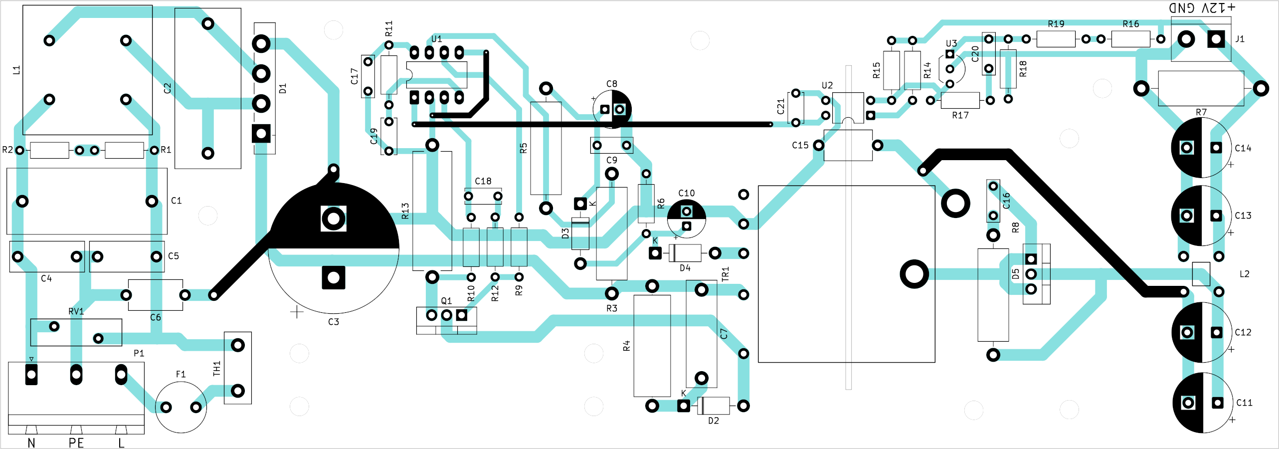
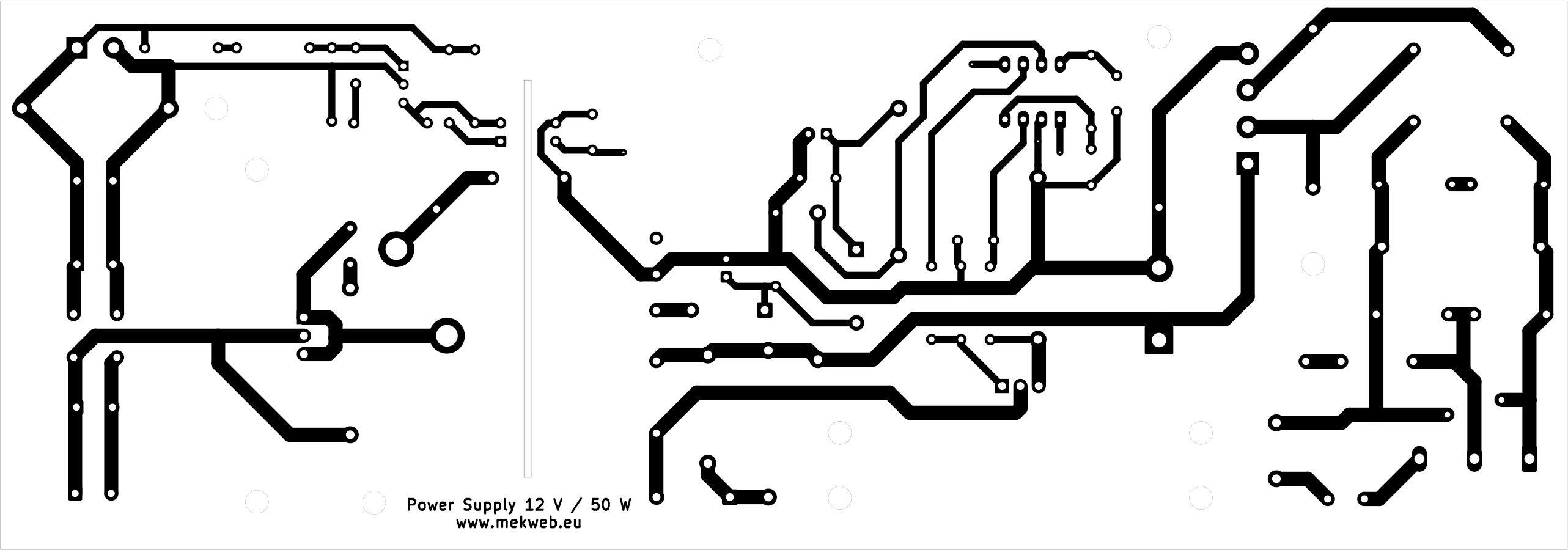
The PCB
Dimensions: 217 x 76 mm. Click on the pictures to get the original size.
Conclusion
By building this power supply I learned something new again, and AI explained and calculated many things for me. First I experimented on a universal PCB (veroboard), and then I designed and made the final PCB, which is published here. After populating it, the supply worked on the first power-up.
The output voltage is a stable 12.1 V and I tested it up to about 4 A (that's 50 W), where the voltage drop was only about 30 mV. I didn't want to go higher in current, I don't have a sufficiently powerful electronic load. But it would probably handle more, up to the point where the overcurrent protection (R13) kicks in. Although the output filter capacitance would likely need to be increased. The supply is quiet, it doesn't whistle and doesn't overheat. The components are recycled, taken from dismantled electronics, so they can once again be used for something useful.
The downloadable file from this page contains some datasheets, as well as the schematic and PCB layout in KiCad format.